G5520A 台湾致新代理商 GMT DC-DC系列 液晶显示器的集成PMIC
| Part Number | Vin (V)min. | Vin (V) max. | FSW (k Hz) | ILX (A) | VLX(V) | OPA S/R (V/us) | OPA ISC (mA) | Note | Package |
| G5520A | 2.5 | 5.5 | 1200 | 1.8 | 20 | 12 | 150 | Async-Boost, VGH/VGL Charge-Pump, VCOM, G5520A With EN, G5520S With XAO |
TQFN3X3-16 |
Bias Power Supply for TFT LCD Panels
General Description The G5520A includes a high-performance boost regu-lator, a VCOM buffer (unity gain OPA), a VGH charge pump driver, and a VGL charge pump driver for ac-tive-matrix thin-film transistor (TFT) liquid-crystal dis-plays (LCDs).
The boost converter provides the regulated supply voltage for the panel source driver ICs. The converter is a high switching frequency (1.2MHz) current mode regulator with an integrated 20V N-Channel 0.7ΩMOSFET that allows the use of ultra-small inductors and ceramic capacitors. It provides fast transient re-sponse to pulsed loading while achieving efficiency over 90%. The device can produce output voltage as high as 18V from an input as low as 2.8V.
The VCOM buffer can drive the LCD VCOM voltage that features high short-circuit current (150mA), fast slew rate (12V/μs), wide bandwidth (12MHz) and rail-to-rail input/output.
A positive and a negative charge-pump driver provide adjustable regulated output voltages VGH and VGL to bias the TFT. Both the charge-pump driver operate with 600kHz switching frequency.
The G5520A includes internal power-up sequencing, over/under voltage protections of the boost converter, and over temperature protection to ensure in safe op-erating.
The G5520A are available in a 16-pin 3X3TQFN packages.
Features
2.5V to 5.5V Input Supply Range
Active-High Enable Control
1.2MHz Current-Mode Boost Regulator
Fast Transient Response to Pulse Load
±1% Accurate Output Voltage
Built-In 20V/1.8A, 0.7ΩN-Channel MOSFET
High Efficiency up to 90%
Over-Current Protection
Output Under-Voltage Protection
High-Performance Operational Amplifier
±150mA Output Short-Circuit Current
12V/μs Slew Rate
12MHz, -3dB Bandwidth
Rail-to-Rail Input and Output
600kHz Negative Charge Pump Driver for VGL
600kHz Positive Charge Pump Driver for VGH
Power-On Sequence Control
Thermal-Overload Protection
TQFN3X3-16 Package
Applications
Photo Frame
GPS
UMPC
Ordering Information
| ORDER NUMBER | MARKING | TEMP. RANGE | PACKAGE (Green) |
| G5520AR41U | 5520A | ~40°C to 85°C | TQFN3X3-16 |
Note:R4:TQFN3X3-16
1: Bonding Code U: Tape & Reel
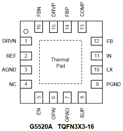
Pin Configuration
台湾GMT致新代理商,欢迎咨询13244774414,还有更多精彩致新电源管理IC分享《致新DC-DC》,《DC-DC芯片》。