G5287 致新代理商 GMT 电源开关及负荷开关系列 1-CH通道电源开关和1-CH通道负载开关 Slew Rate Controlled Load Switch
| Part Number | Vin (V)min. | Vin (V)max. | RON (mΩ) | VOUT Rising (ms) | IOUT(A) | Flag | Dis charge (Ω) | Note | Package |
| G5287 | 1.5 | 5.5 | 80 | 1.00 | / | N | R | External discharging | TDFN1.6X1.6-6 |
General Description
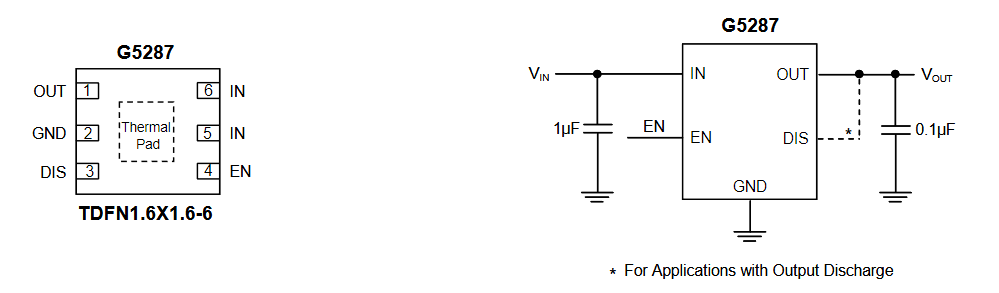
The G5287 is a single P-channel MOSFET power switch designed for high-side load-switching applica-tions. The MOSFET has a typical RDS(ON) of 80mΩ at VCC=5V, allowing increased load switch current han-dling capacity with a low forward voltage drop. The G5287 has a slew rate limited turn-on load switch and offers a shutdown load discharge pin connected to OUT to rapidly turn off a load circuit when the switch is disabled.
The G5287 operates with an input voltage from 1.5V up to 5.5V. It is suitable for 1.8V, 3V and 5V systems. Input logic levels are TTL and 2.5V to 5V CMOS compatible. The typical quiescent supply current is 4μA. In shutdown mode, the supply current decreases to less than 1μA. The G5287 is available in a 6 pin TDFN 1.6X1.6mm package.
Features
- 1.5V to 5.5V Input Voltage Range
- Very Low RDS(ON), Typically 80mΩ (5V)
- Slew Rate Limited Turn-On Time 1ms (5V)
- Fast Load Discharge Pin
- TTL/CMOS Input Logic Level
- TDFN1.6X1.6-6 Package
Applications
- Cellular Telephones
- Digital Still Cameras
- Hot Swap Supplies
- Notebook Computers
- Personal Communication Devices
- Personal Digital Assistants (PDAs)
Ordering Information
| ORDER NUMBER | MARKING | TEMP. RANGE | PACKAGE (Green) |
| 致新G5287RR1U | 5287 | _40°C~ +85°C | TDFN1.6X1.6-6 |
Note: RR: TDFN1.6X1.6-6 1: Bonding Code U: Tape & Reel
Pin Configuration Typical Application Circuit